Concept explainers
Videos
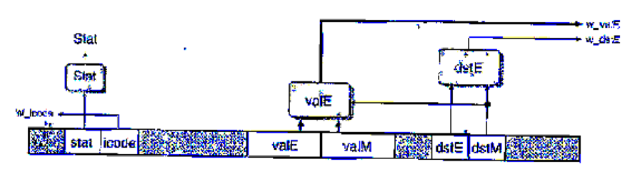
Our pipelined design is a bit unrealistic in that we have two write ports for the register file, but only the popq instruction requires two simultaneous writes to the register file. The other instructions could therefore use a single write port, sharing this for writing valE and valM. The following figure shows a.modified version of the write-back logic, in which we merge the write-back register IDs (W_dstE and W_dstM) into a single signal W_dstE and the write-back values (W_valE and W_yalM) into a single signal w_valE:
The logic for performing the merges is written in HCL as follows:
## Set E port register ID
word w_datE = [
## writing from valM
W_dstH != RNONE : W_dstM;
1: W_dstE;
};
# Set E port value
word w_valE - [
W_dstM != RNONE : W_valM;
1 : W_valE;
};
The control for these multiplexors is determined by dstE—when it indicates there is some register, then it selects the value for port E, and otherwise it selects the value for port M.
In the simulation model, we can then disable register port M, as shown by the following HCL code:
## Disable register port M
## Set M port register ID
word w_dstM = RNONE;
## Set M port value
word w_valM = 0;
The challenge then becomes to devise a way to handle popq. One method is to use the control logic to dynamically process the instruction popq rA so that it has the same effect as the two-instruction sequence
iaddq $8, %rsp
mrmovq -8 (%rsp) , rA
(See Practice Problem 4.3 for a description of the iaddq instruction.) Note the ordering of the two instructions to make sure popq %rsp works properly. You can do this by having the logic in the decode stage treat popq the same as it would the iaddq listed above, exceptthat it predicts the next PC to be equal to the current PC. On the next cycle, the popq instruction is refetched, but the instruction code is converted to a special value IPOP2. This is treated as a special instruction that has the same behavior as the mrmovq instruction listed above.
The file pipe-lw. hcl contains the modified write port logic described above. It contains a declaration of the constant IPOP2 having hexadecimal value E. It also contains the definition of a signal f_icode that generates the (code field for pipeline register D. This definition can be modified to insert the instruction code IPOP2 the second time the popq instruction is fetched. The 1-ICL file also contains a declaration of the signal f_pc, the value of the program counter generated in the fetch stage by the block labeled "Select PC" (Figure 4.57).
Modify the control logic in this the to process popq instructions in the manner we have described. See the lab material for directions on how to generate a simulator for your solution and how to test it.
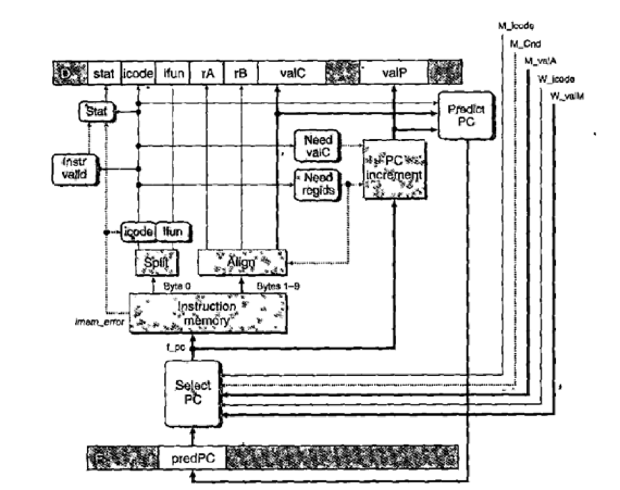
Figure 4.57 PIPE PC selection and fetch logic. Within the one cycle time limit, the processor can only predict the address of the next instruction.
Want to see the full answer?
Check out a sample textbook solution
Chapter 4 Solutions
Computer Systems: A Programmer's Perspective (3rd Edition)
Additional Engineering Textbook Solutions
Starting Out with C++: Early Objects (9th Edition)
Computer Science: An Overview (13th Edition) (What's New in Computer Science)
Web Development and Design Foundations with HTML5 (9th Edition) (What's New in Computer Science)
Starting Out With Visual Basic (7th Edition)
C Programming Language
Starting Out with Java: From Control Structures through Objects (6th Edition)


- (d) The table below shows the ALUcontrol signal of the datapath we discussed in class. Instruction Funct ALU Орсode ALUop ALU action operation field control Iw 00 load word XXXXXX add 0010 Sw 00 store word XXXXXX add 0010 beq 01 branch equal subtract 0110 XXXXXX R-type 10 add 100000 add 0010 R-type 10 subtract 100010 subtract 0110 R-type 10 AND 100100 AND 0000 R-type 10 OR 100101 OR 0001 R-type 10 set on less than 101010 set on less than 0111 You want to add the bne instruction into the datapath, which already includes the required hardware for the instruction. Write out the ALUop for bne and how you can determine whether the bne results in the branch to be taken.arrow_forward1- Write the VHDL code for the circuit shown in figure2. The circuit acts as support circuit for the control unit. It takes 5 bit from a 7 bit bus and start counting down at the rising Bus edge of each clock cycle in case the "Decr" signal is active. A new data loaded to the (4.0) n shift count 5-bit down counter CLK Decr circuit each time the "Ld" signal activated. The output "n" is equal to "1" in case the count value reaches "00000". Explain why the control unit Ld n 04.00 n-0 needs such circuit. Do functional simulation for your design. Figure 2arrow_forwardI believe this problem is from computer systems/architecture. PLEASE TRY YOUR BEST. I NEED TO UNDERSTAND THIS PROBLEM I need you to design a digital logic circuit as a read only memory (ROM) [Decoder + OR gates]. A ROM accepts a three–bit number (x2 x1 x0) and generates an output binary number equal to the input squared + 2. Here is the equation: A = x2 + 2, with input (x) : 0 ≤ (x) ≤ 7 (a) Try to set–up the truth–table [Binary inputs: (x); Binary outputs: ..., A2, A1, A0] (b) What is the size of the initial (unsimplified) ROM ? (c) What is the size of the final (simplified) ROM ?arrow_forward
- The instruction used to fill DX with the its sign bit is: * CWD SAR DX, 1 SAR DX, SF SHR DX, CL SHR DX, SF SAR DX, 10 SAR DX, [SF] SAR DX, 16arrow_forwardDraw the datapath for store instruction. Give clear explanation too.arrow_forwardThe instruction used to copy two bytes from the stack to the Flags Register is: SAHF CMC PUSHF LAHF POPF STC The instruction that can be used to exchange between BL and BH is: * ROL BX, 4 ROL BL, BH ROR BX, 16 ROR BH, BL ROR BX, 8 RCR BX, 8 RCR BL BH To divide the signed number in AX by 2 using shift operations, which instruction should be used: * SAL AX, 1 SHL AX, 2 SAL AX, 2 SHL AX, 1 SHR AX, 1 SHR AX, 2 SAR AX, 1 SAR AX, 2arrow_forward
- How does the width of a register relate to the number of D-flip-flops used in the circuit? Each register is implemented with one D-flip-flop, regardless of the width of the register. Each bit in the register corresponds to two D-flip-flops. Each bit in the register corresponds to a D-flip-flop, so it is 1-to-1. Since D-flip-flops have a Q and Qn output, you only need 1 D-flip-flop for each bit in the register.arrow_forwardDraw the control unit and datapath for the following algorithm that returns an integer value. The function takes two points (x1, y1) and (x2, y2) and computes the equation for a line. It then evaluates and returns ynew for the parameter xp using that line. Use a 16-bit data bus. Show your work; label and clearly mark your diagram. Do not implement this in VHDL. int PredY(int x1, int y1, int x2, int y2, int xp) { int m, b, ynew; if (x1 – x2) <> 0 { m = (y1 - y2) / (x1 - x2); b = y1 - m * x1; ynew = m * xp + b; return(ynew); } else { return(65535); // that's a 16-bit FFFF } }arrow_forwardProblems in this exercise assume that the logic blocks used to implement a processor's datapath (COD Figure 4.23) have the following latencies: Sign HMem/ Register D-Mem File 250 ps 150 ps Mux ALU Adder 25 ps 200 ps 150ps Single Register Register gate Read Setup 5 ps 30ps extend Control 50 ps 20 ps 50ps "Register read" is the time needed after the rising clock edge for the new register value to appear on the output. This value applies to the PC only. "Register setup" is the amount of time a register's data input must be stable before the rising edge of the clock. This value applies to both the PC and Register File. (a) Although the control unit as a whole requires 50 ps, it so happens that we can extract the correct value of the Reg2Loc control wire directly from the instruction. Thus, the value of this control wire is available at the same time as the instruction. Explain how we can extract this value directly from the instruction. Hints: Carefully examine the opcodes shown in COD…arrow_forward
- What happens to the Carry flag when the SHR AX,1 instruction is executed?arrow_forwardWrite the abstract and concrete RTN for the "shr" instruction.arrow_forwardYou need to write in hexadecimal (E.g: OX00114A63) for the following RISC-V assembly instruction: sub ra,gp,t1 * WARNING: You MUST write the Ox followed by the 8 hexadecimal digits all in UPPER case. If needed, add extra zeroes to have the 8 digits (this is auto graded, so no spaces, underscores or lower case). In the previous hexadecimal example Ox00114a63 is incorrect, OX114A63 is also incorrect, and 00114A63 is also incorrect. Only OX00114A63 is correct.arrow_forward
 Database System ConceptsComputer ScienceISBN:9780078022159Author:Abraham Silberschatz Professor, Henry F. Korth, S. SudarshanPublisher:McGraw-Hill Education
 Starting Out with Python (4th Edition)Computer ScienceISBN:9780134444321Author:Tony GaddisPublisher:PEARSON
 Digital Fundamentals (11th Edition)Computer ScienceISBN:9780132737968Author:Thomas L. FloydPublisher:PEARSON
 C How to Program (8th Edition)Computer ScienceISBN:9780133976892Author:Paul J. Deitel, Harvey DeitelPublisher:PEARSON
 Database Systems: Design, Implementation, & Manag...Computer ScienceISBN:9781337627900Author:Carlos Coronel, Steven MorrisPublisher:Cengage Learning
 Programmable Logic ControllersComputer ScienceISBN:9780073373843Author:Frank D. PetruzellaPublisher:McGraw-Hill Education