
(a)
The current
(a)
Answer to Problem 1.41P
- For
- For
Explanation of Solution
Given:
The value of current is,
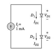
The given circuit is shown below.
Concept Used:
The diode voltage is,
Calculation:
- For,
- For,
From circuit it is clear that,
From circuit it is clear that,
(b)
The current
(b)
Answer to Problem 1.41P
- For
- For
Explanation of Solution
Given:
The value of current is,
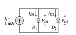
The given circuit is shown below.
Concept Used:
The diode voltage is
Calculation:
- For
- For,
From circuit it is clear that,
From circuit it is clear that,
Since,
Therefore,
So,
Want to see more full solutions like this?
Chapter 1 Solutions
Microelectronics: Circuit Analysis and Design

- 1.6-1 The number In 2 may be calculated from the series In 2 = 1 -+;-+... It is known from analysis that this series converges and that the magnitude of the error in any partial sum is less than the magnitude of the first neglected term. Estimate the number of terms that would be required to calculate In 2 to 10 decimal places.arrow_forwardFor the network shown in figure (3), if the switch is closed for 2usec and then opened for Susec, find mathematical expressions for vi and in of both periods of time and then plot the waveforms of vL and i as a function of time.arrow_forwardConsider the electrical circuit shown in the image. There are 4 currents present. The current I enters a note and then branches into three seperate currents, I1, I2, and I3. A) rank the 4 currents according to their magnitude, greatest first. Explain. B)Considering Delta V1, Delta V2, and Delta V3, now rank them according to magnitude. Explain.arrow_forward
- Obtain numerical values in terms this questionit wants me to express a complex number in polar form, with angle in degrees Please explain this in detail I have confusion with polar form expressionarrow_forwardDetermine the time constant T1 of circuit R1C1arrow_forwardI am having problems with solving the integral for parts C and D if you could help. See copy pasted full question 1.25. The book information is also below. Also see attached figure. The chegg solution doesnt explain good enough. I attached the chegg soluiton with with the part I dont understand circled in red. Book: Electric Circuits 10th Edition by James W. Nilsson Susan Riedel 1.25 The voltage and current at the terminals of the element in Fig. 1.5 are v = 250 cos 800pt V, i = 8 sin 800pt A. a) Find the maximum value of the power being delivered to the element. b) Find the maximum value of the power being extracted from the element. c) Find the average value of p in the interval d) Find the average value of p in the interval See attached for Fig. 1.5arrow_forward
- For the circuit in Figure: 1) Set up the equation for the upper supermesh. Response format: Ai1 ± Bi2 ± Ci3 ± Di4 = E 2) Set up the auxiliary equation for the top supermesh. Response format: Ai1 ± Bi2 ± Ci3 ± Di4 = E 3) Set up the equation for the lower supermesh. Response format: Ai1 ± Bi2 ± Ci3 ± Di4 = E 4) Set up the auxiliary equation for the lower supermesh. Response format: Ai1 ± Bi2 ± Ci3 ± Di4 = E 5) What is the value of ix in A?arrow_forwardR2(Rx+Rnp)=R1(R3+Rnp)........(2) Rnp/Rmp=R1/R2.........(1) Substitute equation 2 into equation 1arrow_forward2 The figure is a graph of ... 5 (5 Points) Current Voltage the current across a voltage as a function of the potential difference through it the resistance as a function of the current across a component the current through a component as a function of the voltage across it All three of the above (a), (b), and (c) are true None of the above (a), (b), or (c) is truearrow_forward
 Introductory Circuit Analysis (13th Edition)Electrical EngineeringISBN:9780133923605Author:Robert L. BoylestadPublisher:PEARSON
 Delmar's Standard Textbook Of ElectricityElectrical EngineeringISBN:9781337900348Author:Stephen L. HermanPublisher:Cengage Learning
 Programmable Logic ControllersElectrical EngineeringISBN:9780073373843Author:Frank D. PetruzellaPublisher:McGraw-Hill Education
 Fundamentals of Electric CircuitsElectrical EngineeringISBN:9780078028229Author:Charles K Alexander, Matthew SadikuPublisher:McGraw-Hill Education
 Electric Circuits. (11th Edition)Electrical EngineeringISBN:9780134746968Author:James W. Nilsson, Susan RiedelPublisher:PEARSON
 Engineering ElectromagneticsElectrical EngineeringISBN:9780078028151Author:Hayt, William H. (william Hart), Jr, BUCK, John A.Publisher:Mcgraw-hill Education,