Concept explainers
Design a problem to provide better understanding regarding transistors.
Explanation of Solution
Given data:
Refer Figure 3.128 in the textbook for the transistor circuit.
Formula used:
Write the expression for collector current in transistor.
Here,
Calculation:
Let us assume that the value of resistance
The given circuit with the assumed value is shown in Figure 1.
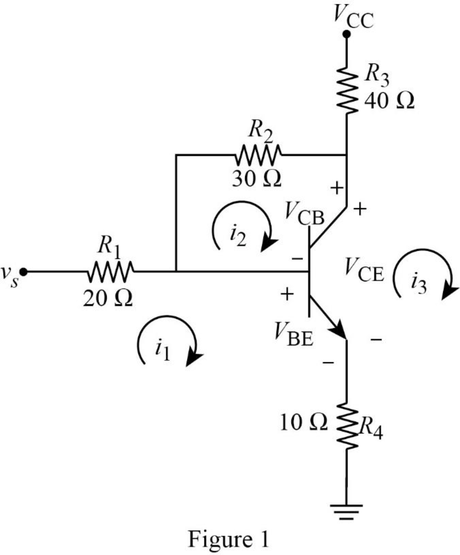
Apply Kirchhoff’s voltage law to loop 1 with current
Substitute
Apply Kirchhoff’s voltage law to loop 2 with current
Apply Kirchhoff’s voltage law to output loop in Figure 1.
Write the constraint equations.
Substitute equations (5) and (6) in (1).
Substitute
Rearrange equation (7).
Substitute equation (9) in (3).
Substitute
Substitute equation (8) in (2).
Substitute equation (10) in (11).
Substitute equation (10) and (12) in (8).
Substitute equation (12) and (13) in (4).
Simplify the equation as follows.
Conclusion:
Therefore, the problem has been designed to provide better understanding regarding transistors.
Want to see more full solutions like this?
Chapter 3 Solutions
Fundamentals of Electric Circuits


- -8V R=1.2k2 %3D +12V R2= 2-5k2 Silicondiode रिह %3D Construct the circuit in more easy way and kindly solve the following thank you withexplanation please Diode condition * current * Diade current li0) * Diode voltage (vo) * Output voltage ( )arrow_forward2. For the circuit of Fig. 3.54 (which is a model for the de operation of a bipolar junction transistor biased in forward active region), IB is measured to be 100 LA. Determine Ic and Ig. 1 kN R1 IB 150/g R2 1 k2 FIGURE 3.54arrow_forwardFor the transistor shown below B=hfe = hfe = 150, VBE =0.7V, and VT= 25mV. All capacitors are ideal. Calculate vo. I kQ ww I k2 ww 100 k2 ww 100 k2 16 V 16 V 2 V ww 200 k£2 2 V 200 k2arrow_forward
- Find Ig, Ic, and v, in the transistor circuit of Fig. 3.41. Assume that the transistor operates in the active mode and that B = 50. Ic 100 2 ww 20 k2 6 V Output loop + VBE 4 V Input loop Figure 3.41arrow_forward3.32. While constructing a full-wave rectifier, a student mistakenly has swapped the termi- nals of D3 as depicted in Fig. 3.82. Explain what happens. D2. D3 * Vout + Vin RL DA Figure 3.82arrow_forwardFor the transistor in circuit shown below. 3 = 200. +6 V 10 ka Va 1 k2 If V, = 0 V, the value of I, and V, are (A) 6.43 mA, 2.4 V (B) 2.18 mA, 3.4 V (C) 0 A, 6 V (D) None of thesearrow_forward
- 3.68 A digital circuit is required to display a digital signal on a bar-graph LED, similar to a sound meter on a stereo. You know that the input to your circuit has values from 0 to 3 coded in binary format. You need to indicate the value in a bar graph where pro- gressively more LEDs turn on as the input number gets higher, as shown in Fig- ure 3.120. When the highest number is reached, all LEDs are on. a. Write the truth table for the circuit required to drive the LEDs. Assume that the inputs are called D₁ and Do and the outputs are Y₁, Y₂, and Y3, where Y₁ is the low- est LED in the diagram in Figure 3.120 and Y3 is the highest. Assume that the out- puts are active-HIGH. b. Write and simplify the Boolean equations for the three outputs. Draw a logic cir- cuit to show how the simplified functions can be implemented. Y₂ D₁ Do = 00 FIGURE 3.120 Problem 3.68: Bar-Graph LED 01 10 11arrow_forwardKnow how to design simple voltage-divider and currentdivider circuits What is the maximum power dissipated in the 75 kΩ resistor?arrow_forwardD,on B2. 3.40. We wish to design a circuit that exhibits the input/output characteristic shown in Fig. 3.83. Using 1-k2 resistors, ideal diodes, and other components, construct the circuit. Vout + 2 V 0.5 -2 V + 2 V Vin -2 V 0.5 Figure 3.83arrow_forward
- The terminal voltage of a battery is 13.5 v when 5 A current enters its positive terminal, but when a 5 A current leaves its positive terminal, the terminal voltage becomes 11.5 v. Determine the EMF and internal resistance of this battery. (8 = ?, r =?)arrow_forwardQuèstion 3 For the following circuit, as we increase the load resistance R, the diode current Ip increases. Ip tVD- Vs 3RL True False Moving to another question will save this response. Ciparrow_forwardQuestion 3.28 An input voltage of 2V rms (measured from base to ground) is applied to the circuit of Fig. 3.21. Its putting that the emitter voltage follows the base voltage exactly and that Vbe (rms)= 0.1 V, Calculate the voltage amplification of the circuit (AV= V0/Vi) and the emitter current for RE= 1kilohms.arrow_forward
 Introductory Circuit Analysis (13th Edition)Electrical EngineeringISBN:9780133923605Author:Robert L. BoylestadPublisher:PEARSON
 Delmar's Standard Textbook Of ElectricityElectrical EngineeringISBN:9781337900348Author:Stephen L. HermanPublisher:Cengage Learning
 Programmable Logic ControllersElectrical EngineeringISBN:9780073373843Author:Frank D. PetruzellaPublisher:McGraw-Hill Education
 Fundamentals of Electric CircuitsElectrical EngineeringISBN:9780078028229Author:Charles K Alexander, Matthew SadikuPublisher:McGraw-Hill Education
 Electric Circuits. (11th Edition)Electrical EngineeringISBN:9780134746968Author:James W. Nilsson, Susan RiedelPublisher:PEARSON
 Engineering ElectromagneticsElectrical EngineeringISBN:9780078028151Author:Hayt, William H. (william Hart), Jr, BUCK, John A.Publisher:Mcgraw-hill Education,