
Microelectronics: Circuit Analysis and Design
4th Edition
ISBN: 9780073380643
Author: Donald A. Neamen
Publisher: McGraw-Hill Companies, The
expand_more
expand_more
format_list_bulleted
Videos
Textbook Question
Chapter 16, Problem 16.27P
What is the logic function implemented by the circuit in Figure P16.27.
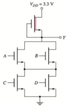
Figure P16.27
Expert Solution & Answer
Want to see the full answer?
Check out a sample textbook solution
Students have asked these similar questions
(a) Consider a combinational logic circuit in Figure Q.2 (a).i and Q.2 (a).ii. Determine the
Boolean equation for the output Y and then, replace the circuit with a single logic gate.
Figure Q.2 (a)i
Vpp
Voo
Figure Q.2 (a)ii
(a)
Discuss the key characteristics of Unipolar Logic Families and Bipolar Logic Families.
What points are important to consider for interfacing the components from different
Logic Families.
(a) Find VH and VL for the Schottky DTL gateshown. (b) What are the input currents in thetwo logic states? (c) What is the fanout of the gate?
Chapter 16 Solutions
Microelectronics: Circuit Analysis and Design
Ch. 16 - Consider the NMOS inverter with resistor load in...Ch. 16 - The enhancementload NMOS inverter in Figure...Ch. 16 - Prob. 16.3EPCh. 16 - Prob. 16.4EPCh. 16 - Consider the NMOS inverter with enhancement load,...Ch. 16 - Prob. 16.2TYUCh. 16 - (a) Consider the results of Exercise Ex 16.1....Ch. 16 - Prob. 16.5EPCh. 16 - Prob. 16.6EPCh. 16 - (a) Design a threeinput NMOS NOR Logic gate with...
Ch. 16 - Consider the NMOS logic circuit in Figure 16.18....Ch. 16 - Repeat Exercise TYU 16.5 for the NMOS logic...Ch. 16 - The CMOS inverter in Figure 16.21 is biased at...Ch. 16 - swA CMOS inverter is biased at VDD=3V . The...Ch. 16 - A CMOS inverter is biased at VDD=1.8V . The...Ch. 16 - Prob. 16.7TYUCh. 16 - Repeat Exercise Ex 16.9 for a CMOS inverter biased...Ch. 16 - Determine the transistor sizes of a 3input CMOS...Ch. 16 - Design the widthtolength ratios of the transistors...Ch. 16 - Design a static CMOS logic circuit that implements...Ch. 16 - Prob. 16.10TYUCh. 16 - Prob. 16.11TYUCh. 16 - Sketch a clocked CMOS logic circuit that realizes...Ch. 16 - Prob. 16.12EPCh. 16 - Prob. 16.13TYUCh. 16 - Consider the CMOS transmission gate in Figure...Ch. 16 - Prob. 16.15TYUCh. 16 - Prob. 16.14EPCh. 16 - Prob. 16.16TYUCh. 16 - Prob. 16.17TYUCh. 16 - Sketch the quasistatic voltage transfer...Ch. 16 - Sketch an NMOS threeinput NOR logic gate. Describe...Ch. 16 - Discuss how more sophisticated (compared to the...Ch. 16 - Sketch the quasistatic voltage transfer...Ch. 16 - Discuss the parameters that affect the switching...Ch. 16 - Prob. 6RQCh. 16 - Sketch a CMOS threeinput NAND logic gate. Describe...Ch. 16 - sDiscuss how more sophisticated (compared to the...Ch. 16 - Prob. 9RQCh. 16 - Sketch an NMOS transmission gate and describe its...Ch. 16 - Sketch a CMOS transmission gate and describe its...Ch. 16 - Discuss what is meant by pass transistor logic.Ch. 16 - Prob. 13RQCh. 16 - Prob. 14RQCh. 16 - Prob. 15RQCh. 16 - Describe the basic architecture of a semiconductor...Ch. 16 - ‘Sketch a CMOS SRAM cell and describe its...Ch. 16 - Prob. 18RQCh. 16 - Describe a maskprogrammed MOSFET ROM memory.Ch. 16 - Describe the basic operation of a floating gate...Ch. 16 - Prob. 16.1PCh. 16 - Prob. 16.2PCh. 16 - (a) Redesign the resistive load inverter in Figure...Ch. 16 - Prob. D16.4PCh. 16 - Prob. 16.5PCh. 16 - Prob. D16.6PCh. 16 - Prob. 16.7PCh. 16 - Prob. 16.8PCh. 16 - For the depletion load inverter shown in Figure...Ch. 16 - Prob. 16.10PCh. 16 - Prob. D16.11PCh. 16 - Prob. D16.12PCh. 16 - Prob. 16.13PCh. 16 - For the two inverters in Figure P16.14, assume...Ch. 16 - Prob. 16.15PCh. 16 - Prob. 16.16PCh. 16 - Prob. 16.17PCh. 16 - Prob. 16.18PCh. 16 - Prob. D16.19PCh. 16 - Prob. 16.20PCh. 16 - Prob. 16.21PCh. 16 - Prob. 16.22PCh. 16 - In the NMOS circuit in Figure P16.23, the...Ch. 16 - Prob. 16.24PCh. 16 - Prob. 16.25PCh. 16 - Prob. 16.26PCh. 16 - What is the logic function implemented by the...Ch. 16 - Prob. D16.28PCh. 16 - Prob. D16.29PCh. 16 - Prob. 16.31PCh. 16 - Prob. 16.32PCh. 16 - Prob. 16.33PCh. 16 - Consider the CMOS inverter pair in Figure P16.34....Ch. 16 - Prob. 16.35PCh. 16 - Prob. 16.36PCh. 16 - Prob. 16.37PCh. 16 - Prob. 16.38PCh. 16 - Prob. 16.39PCh. 16 - (a) A CMOS digital logic circuit contains the...Ch. 16 - Prob. 16.41PCh. 16 - Prob. 16.42PCh. 16 - Prob. 16.43PCh. 16 - Prob. 16.44PCh. 16 - Prob. 16.45PCh. 16 - Prob. 16.46PCh. 16 - Prob. 16.47PCh. 16 - Prob. 16.48PCh. 16 - Prob. 16.49PCh. 16 - Prob. 16.50PCh. 16 - Prob. 16.51PCh. 16 - Prob. 16.52PCh. 16 - Prob. D16.53PCh. 16 - Figure P16.54 is a classic CMOS logic gate. (a)...Ch. 16 - Figure P16.55 is a classic CMOS logic gate. (a)...Ch. 16 - Consider the classic CMOS logic circuit in Figure...Ch. 16 - (a) Given inputs A,B,C,A,B and C , design a CMOS...Ch. 16 - (a) Given inputs A, B, C, D, and E, design a CMOS...Ch. 16 - (a) Determine the logic function performed by the...Ch. 16 - Prob. D16.60PCh. 16 - Prob. 16.61PCh. 16 - Prob. 16.62PCh. 16 - Sketch a clocked CMOS domino logic circuit that...Ch. 16 - Sketch a clocked CMOS domino logic circuit that...Ch. 16 - Prob. D16.65PCh. 16 - Prob. 16.66PCh. 16 - Prob. 16.67PCh. 16 - The NMOS transistors in the circuit shown in...Ch. 16 - Prob. 16.69PCh. 16 - Prob. 16.70PCh. 16 - Prob. 16.71PCh. 16 - (a) Design an NMOS pass transistor logic circuit...Ch. 16 - Prob. 16.73PCh. 16 - What is the logic function implemented by the...Ch. 16 - Prob. 16.75PCh. 16 - Prob. 16.76PCh. 16 - Prob. 16.77PCh. 16 - Consider the NMOS RS flipflop in Figure 16.63...Ch. 16 - Prob. 16.79PCh. 16 - Consider the circuit in Figure P16.80. Determine...Ch. 16 - Prob. D16.81PCh. 16 - Prob. 16.82PCh. 16 - Prob. 16.83PCh. 16 - Prob. 16.84PCh. 16 - (a) A 1 megabit memory is organized in a square...Ch. 16 - Prob. 16.86PCh. 16 - Prob. 16.87PCh. 16 - Prob. 16.88PCh. 16 - Prob. D16.89PCh. 16 - Prob. 16.90PCh. 16 - Prob. 16.91PCh. 16 - Prob. 16.92PCh. 16 - Prob. D16.93PCh. 16 - Prob. D16.94PCh. 16 - Prob. D16.95PCh. 16 - An analog signal in the range 0 to 5 V is to be...Ch. 16 - Prob. 16.97PCh. 16 - Prob. 16.98PCh. 16 - Prob. 16.99PCh. 16 - The weightedresistor D/A converter in Figure 16.90...Ch. 16 - The Nbit D/A converter with an R2R ladder network...Ch. 16 - Prob. 16.102PCh. 16 - Prob. 16.103PCh. 16 - Prob. 16.104PCh. 16 - Prob. 16.105PCh. 16 - Design a classic CMOS logic circuit that will...Ch. 16 - Prob. D16.111DPCh. 16 - Prob. D16.112DPCh. 16 - Prob. D16.113DP
Knowledge Booster


Learn more about
Need a deep-dive on the concept behind this application? Look no further. Learn more about this topic, electrical-engineering and related others by exploring similar questions and additional content below.Similar questions
- A) Starting from Ex-OR (SOP) expression: a- develop Ex-NOR (SOP) expression. A OA=.. b- Find AO 1=..., B) Draw the logic circuit diagram for 4x1 Multiplexer.arrow_forwardDraw the logic diagram and transistor implementation for a (2-2-2) AOI.arrow_forward(a) Construct an Inverter Logic Gate using both TTL and CMOS Logic Family.arrow_forward
- (e) Describe, with the help of sketches, the definition and meaning of noise margins in an inverter logic gate.arrow_forwardWhat is a TTL circuit? What are their main characteristics? (Input voltage and current, output voltage and current, Vcc, …)arrow_forwardQ2 A) Starting from Ex-OR (SOP) expression: a- develop Ex-NOR (SOP) expression. A O A=.... b- Find AO 1=..., B) Draw the logic circuit diagram for 4x1 Multiplexer.arrow_forward
- We need to implement digital logic function Y = A(B + C(D + E)). a) Design a CMOS logic gate to implement. b) Design a TTL logic gate to implement.arrow_forwardSatisfy the given table using CMOS Logic. Write a clear logic diagram and label the inputs properly.arrow_forwardInverters create an ac voltage when only a dc voltage source is available. Select one: O a. True O b. None of the above O c. False Jump to...arrow_forward
arrow_back_ios
SEE MORE QUESTIONS
arrow_forward_ios
Recommended textbooks for you

Introduction to Logic Gates; Author: Computer Science;https://www.youtube.com/watch?v=fw-N9P38mi4;License: Standard youtube license