
Videos
The NMOS transistors in the circuit shown in Figure P16.68 have parameters
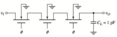
Figure P16.68
Want to see the full answer?
Check out a sample textbook solution
Chapter 16 Solutions
Microelectronics: Circuit Analysis and Design


- 1. A SCR has a forward breakover voltage of 175V when a gate pulse of 2 mA is made to flow. Find the conduction angle if a sinusoidal voltage of 350 V peak is applied.arrow_forwardState whether the following statement is true or false. “The curvature in the output voltage of a bandgap reference circuit occurs mainly due to the non-linearity in the PTAT current.”arrow_forwardVLSI Wafer Yield Given the defect density D= and chip area A, use Murphy's yield model to estimate the chip yield. Calculate for D=0.5 defects/cm2 D=0.5 defects/cm2 and A=1.5 cm2 A=1.5 cm2.arrow_forward
- Write true or false for each statement 1) Phosphorous ions are implanted into active areas of NMOS transistors. 2) P-well is required for PMOS transistors if lightly doped p-type silicon wafer is used as a substrate. 3) Silicon dioxide is a very good conductor like metal 1 layer. 4) Aluminum is used for making a gate terminal on top of a SiO2 layer in CMOS fabrication. 5) Photolithography is a process of implanting atoms into the silicon substrate to make transistors.arrow_forwardQ/ for square wave PWM inverter, Vdc=100V, L=25mH, R=10Ω, f=60Hz. draw the spectrum of the output voltage and current and then find the rms current value and the output power. Take n =1-20.arrow_forward2&cmid%3D11818 SThis course Assume Is = 8 x 10¹⁶ A, B = 200, and VA =. For the circuit shown below, and assuming IE=lc, the value of r is %3D Vcc=2 V 1 mA Select one: Oa. None of these O b. 3.9 KO O c. 2.6 KO O d. 5.2 KQ An NPN transistor having a current gain B = 120, is biased to get a collector current Ic= 1 mA, if VA = 150 V. and V mV, then its transconductance gm - and ro =arrow_forward
- For Enhancement type nMOS transistor , derive the following expression ID = μnCox/2 W/L (VGS-Vt)2(1+ λVDS)arrow_forward2. Assuming B= 100, Calcu;late lc, Ve, Vc and Vce in figure below? %3D +15 V 10 k 15 k 12 k -25 V Determine the Q point and load line endpoints of the circuit and Plot the Q point (Ic and VCE) on the load line for the circuit.arrow_forward1) what is the Voltage & Current rating ofTriode for Alternating Current (TRIAC) 2) 5. Are the following statements correct or wrong? Justify your answer.(a) Thyristors are used only for low voltage, low current applications.(b) MOSFETs are used for high frequency applications.(c) BJT is more efficient than IGBT in high power applications.(d) GTO requires very low current applied to its gate to be turn off.(e) IGBT is a voltage driven device.arrow_forward
- FET Construction 1. In the depletion type MOSFET there are two modes of operation : 1 2 2. In an n-channel enhancement type MOSFET if VGS = OV and VDS > Ov then ID >0 A. a) True. b) False. (if false correct the answer) 3. When a negative potential is applied to the gate terminal of a depletion type MOSFET transistor, the number of free carriers at the channel are 4. In an n-channel depletion type MOSFET consider the situation if VGS is kept constant and Vos is increased. Explain briefly what will happen to the channel if Vos is increased further. 5. In an n-channel enhancement type MOSFET if VDs ≥ VGS - Vth and VGS Vth then Ip 6. In an enhancement type MOSFET if: a) VGs > Vth and Vos = Ov then the shape of the channel is b) VGS > Vth and VDs > Ov then the shape of the channel is 7. In an n-channel depletion type MOSFET V, is a p-channel depletion type MOSFET V₁ is while forarrow_forwardA single-phase full bridge inverter is fed for a dc source such that fundamental component of output voltage is 230 V. The input frequency is 50 Hz. Find the rms value of MOSFET and diode currents if load is RLC: R=2 0, L=19 mH, and C=400 µF.arrow_forwardONLY NEED Q17, Q16 mentioned because it is relevant to Q17 Q17.In the above example, find (i) emitter voltage w.r.t. ground (ii) base voltage w.r.t. ground (iii) collector voltage w.r.t. ground. Q16.Determine the Q point of the transistor circuit shown in the figure. Also draw the d.c. load line. Given β = 200 and VBE = 0.7V.arrow_forward
 Introductory Circuit Analysis (13th Edition)Electrical EngineeringISBN:9780133923605Author:Robert L. BoylestadPublisher:PEARSON
 Delmar's Standard Textbook Of ElectricityElectrical EngineeringISBN:9781337900348Author:Stephen L. HermanPublisher:Cengage Learning
 Programmable Logic ControllersElectrical EngineeringISBN:9780073373843Author:Frank D. PetruzellaPublisher:McGraw-Hill Education
 Fundamentals of Electric CircuitsElectrical EngineeringISBN:9780078028229Author:Charles K Alexander, Matthew SadikuPublisher:McGraw-Hill Education
 Electric Circuits. (11th Edition)Electrical EngineeringISBN:9780134746968Author:James W. Nilsson, Susan RiedelPublisher:PEARSON
 Engineering ElectromagneticsElectrical EngineeringISBN:9780078028151Author:Hayt, William H. (william Hart), Jr, BUCK, John A.Publisher:Mcgraw-hill Education,