
Microelectronics: Circuit Analysis and Design
4th Edition
ISBN: 9780073380643
Author: Donald A. Neamen
Publisher: McGraw-Hill Companies, The
expand_more
expand_more
format_list_bulleted
Videos
Textbook Question
Chapter 3, Problem 3.30P
Consider the circuit in Figure P3.30. The transistor parameters are
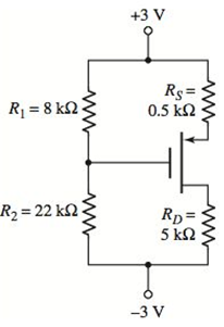
Figure P3.30
Expert Solution & Answer
Want to see the full answer?
Check out a sample textbook solution
Students have asked these similar questions
Determine vo versus v₁ for the circuit shown in Figure 2. Assume that
the MOSFET operates in saturation and is characterized by the parameters K and VT.
Vs
R₁
www
Figure 2
wwww
RL
R₂
wwwww VO
Note: assuming the MOSFET works at normal saturation regime and
ips= (VDS -VT)²2
K
2
Design the following MOSFET circuit for it
to operate in saturation mode with 0.5 mA
drain current. Determine Rp and dc
voltage VĎ. Assume V₁ = 2 V and K = 0.1
mA/V² for this MOSFET.
10 V
RD
-VD
For the PN junction under sun light, the short circuit current amount is Isc. Please sketch
the I-V curve of PN under the sun based on that under the dark condition above. Indicate
Isc and Voc in your plot.
Chapter 3 Solutions
Microelectronics: Circuit Analysis and Design
Ch. 3 - An NMOS transistor with VTN=1V has a drain current...Ch. 3 - An PMOS device with VTP=1.2V has a drain current...Ch. 3 - (a) An nchannel enhancementmode MOSFET has a...Ch. 3 - The NMOS devices described in Exercise TYU 3.1...Ch. 3 - (a) A pchannel enhancementmode MOSFET has a...Ch. 3 - The PMOS devices described in Exercise TYU 3.3...Ch. 3 - The parameters of an NMOS enhancementmode device...Ch. 3 - An NMOS transistor has parameters VTNO=0.4V ,...Ch. 3 - Prob. 3.3EPCh. 3 - The transistor in Figure 3.26(a) has parameters...
Ch. 3 - For the transistor in the circuit in Figure 3.28,...Ch. 3 - Consider the circuit shown in Figure 3.30. The...Ch. 3 - Consider the circuit in Figure 3.30. Using the...Ch. 3 - (a) Consider the circuit shown in Figure 3.33. The...Ch. 3 - Consider the NMOS inverter shown in Figure 3.36...Ch. 3 - Consider the circuit shown in Figure 3.39 with...Ch. 3 - Consider the circuit in Figure 3.41. Assume the...Ch. 3 - Prob. 3.7TYUCh. 3 - Consider the circuit in Figure 3.43. The...Ch. 3 - For the circuit shown in Figure 3.36, use the...Ch. 3 - Consider the circuit shown in Figure 3.44. The...Ch. 3 - For the circuit shown in Figure 3.39, use the...Ch. 3 - For the MOS inverter circuit shown in Figure 3.45,...Ch. 3 - For the circuit in Figure 3.46, assume the circuit...Ch. 3 - The circuit shown in Figure 3.45 is biased at...Ch. 3 - The transistor in the circuit shown in Figure 3.48...Ch. 3 - In the circuit in Figure 3.46, let RD=25k and...Ch. 3 - For the circuit shown in Figure 3.49(a), assume...Ch. 3 - Prob. 3.15EPCh. 3 - Consider the constantcurrent source shown in...Ch. 3 - Consider the circuit in Figure 3.49(b). Assume...Ch. 3 - Consider the circuit shown in Figure 3.50. Assume...Ch. 3 - The transistor parameters for the circuit shown in...Ch. 3 - The transistor parameters for the circuit shown in...Ch. 3 - The parameters of an nchannel JFET are IDSS=12mA ,...Ch. 3 - The transistor in the circuit in Figure 3.62 has...Ch. 3 - For the pchannel transistor in the circuit in...Ch. 3 - Consider the circuit shown in Figure 3.66 with...Ch. 3 - The nchannel enhancementmode MESFET in the circuit...Ch. 3 - For the inverter circuit shown in Figure 3.68, the...Ch. 3 - Describe the basic structure and operation of a...Ch. 3 - Sketch the general currentvoltage characteristics...Ch. 3 - Describe what is meant by threshold voltage,...Ch. 3 - Describe the channel length modulation effect and...Ch. 3 - Describe a simple commonsource MOSFET circuit with...Ch. 3 - Prob. 6RQCh. 3 - In the dc analysis of some MOSFET circuits,...Ch. 3 - Prob. 8RQCh. 3 - Describe the currentvoltage relation of an...Ch. 3 - Describe the currentvoltage relation of an...Ch. 3 - Prob. 11RQCh. 3 - Describe how a MOSFET can be used to amplify a...Ch. 3 - Describe the basic operation of a junction FET.Ch. 3 - Prob. 14RQCh. 3 - (a) Calculate the drain current in an NMOS...Ch. 3 - The current in an NMOS transistor is 0.5 mA when...Ch. 3 - The transistor characteristics iD versus VDS for...Ch. 3 - For an nchannel depletionmode MOSFET, the...Ch. 3 - Verify the results of Example 3.4 with a PSpice...Ch. 3 - The threshold voltage of each transistor in Figure...Ch. 3 - The threshold voltage of each transistor in Figure...Ch. 3 - Consider an nchannel depletionmode MOSFET with...Ch. 3 - Determine the value of the process conduction...Ch. 3 - An nchannel enhancementmode MOSFET has parameters...Ch. 3 - Consider the NMOS circuit shown in Figure 3.36....Ch. 3 - An NMOS device has parameters VTN=0.8V , L=0.8m ,...Ch. 3 - Consider the NMOS circuit shown in Figure 3.39....Ch. 3 - A particular NMOS device has parameters VTN=0.6V ,...Ch. 3 - MOS transistors with very short channels do not...Ch. 3 - For a pchannel enhancementmode MOSFET, kp=50A/V2 ....Ch. 3 - For a pchannel enhancementmode MOSFET, the...Ch. 3 - The transistor characteristics iD versus SD for a...Ch. 3 - A pchannel depletionmode MOSFET has parameters...Ch. 3 - Calculate the drain current in a PMOS transistor...Ch. 3 - sDetermine the value of the process conduction...Ch. 3 - Enhancementmode NMOS and PMOS devices both have...Ch. 3 - For an NMOS enhancementmode transistor, the...Ch. 3 - The parameters of an nchannel enhancementmode...Ch. 3 - An enhancementmode NMOS transistor has parameters...Ch. 3 - An NMOS transistor has parameters VTO=0.75V ,...Ch. 3 - (a) A silicon dioxide gate insulator of an MOS...Ch. 3 - In a power MOS transistor, the maximum applied...Ch. 3 - In the circuit in Figure P3.26, the transistor...Ch. 3 - The transistor in the circuit in Figure P3.27 has...Ch. 3 - Prob. D3.28PCh. 3 - The transistor in the circuit in Figure P3.29 has...Ch. 3 - Consider the circuit in Figure P3.30. The...Ch. 3 - For the circuit in Figure P3.31, the transistor...Ch. 3 - Design a MOSFET circuit in the configuration shown...Ch. 3 - Consider the circuit shown in Figure P3.33. The...Ch. 3 - The transistor parameters for the transistor in...Ch. 3 - For the transistor in the circuit in Figure P3.35,...Ch. 3 - Design a MOSFET circuit with the configuration...Ch. 3 - The parameters of the transistors in Figures P3.37...Ch. 3 - For the circuit in Figure P3.38, the transistor...Ch. 3 - Prob. 3.39PCh. 3 - Prob. 3.40PCh. 3 - Design the circuit in Figure P3.41 so that...Ch. 3 - Prob. 3.42PCh. 3 - Prob. 3.43PCh. 3 - Prob. 3.44PCh. 3 - Prob. 3.45PCh. 3 - Prob. 3.46PCh. 3 - Prob. 3.47PCh. 3 - The transistors in the circuit in Figure 3.36 in...Ch. 3 - For the circuit in Figure 3.39 in the text, the...Ch. 3 - Prob. 3.50PCh. 3 - The transistor in the circuit in Figure P3.51 is...Ch. 3 - Prob. 3.52PCh. 3 - For the twoinput NMOS NOR logic gate in Figure...Ch. 3 - All transistors in the currentsource circuit shown...Ch. 3 - All transistors in the currentsource circuit shown...Ch. 3 - Consider the circuit shown in Figure 3.50 in the...Ch. 3 - The gate and source of an nchannel depletionmode...Ch. 3 - For an nchannel JFET, the parameters are IDSS=6mA...Ch. 3 - A pchannel JFET biased in the saturation region...Ch. 3 - Prob. 3.60PCh. 3 - Prob. 3.61PCh. 3 - The threshold voltage of a GaAs MESFET is...Ch. 3 - Prob. 3.63PCh. 3 - Prob. 3.64PCh. 3 - Prob. 3.65PCh. 3 - For the circuit in Figure P3.66, the transistor...Ch. 3 - Prob. 3.67PCh. 3 - Prob. 3.68PCh. 3 - For the circuit in Figure P3.69, the transistor...Ch. 3 - Prob. 3.70PCh. 3 - Prob. 3.71PCh. 3 - Prob. 3.72PCh. 3 - Using a computer simulation, verify the results of...Ch. 3 - Consider the PMOS circuit shown in Figure 3.30....Ch. 3 - Consider the circuit in Figure 3.39 with a...Ch. 3 - Prob. D3.79DPCh. 3 - Consider the multitransistor circuit in Figure...
Knowledge Booster


Learn more about
Need a deep-dive on the concept behind this application? Look no further. Learn more about this topic, electrical-engineering and related others by exploring similar questions and additional content below.Similar questions
- Set up a midpoint bias for a JFET with IDSS = 14 mA and VGS(off) = -10 V. Use a 24 V dc source as the supply voltage. Show the circuit and resistor values. Indicate the value of ID. Indicate the value of VGS. Indicate the value of VDS.arrow_forwardIdentify the source, drain, gate, and bulk terminalsand find the current I in the transistorsAssume VTN = 0.70 Varrow_forwardDetermine VB, VE, VC, VCE, IB, IE, and IC in Figure. The 2N3904 is a general purpose transistor with a typical BDC 200 Vcc +30 V WWII VCE VB R₁ • 22 ΚΩ IC(mA) Chọn... * Chọn... * IB(UA) Chọn... * IE(MA) Chọn... ◆ Chọn... * Chọn... * Chọn... * VE VC R₂ ´ 10 ΚΩ www Rc 1.0 ΚΩ 2N3904 PDC=200 RE 1.0 ΚΩarrow_forward
- A transistor has the CB input characteristics shown in Figure 3–11 (p. 106 ). If alpha = 0.95, find IC when VBE = 0.72 V and VCB = 10 V.arrow_forward3. Write down which transistor structure each curve characteristic belongs to in the figure. Ip -VGS -VGS +VGs (c) VGS (b) (a)arrow_forwardFigure 1 shows the typical output characteristics of MOSFET. Those characteristics show the difference curve of the drain current, Ip, as function of the drain- source voltage, VDs at a given gate-source voltage, VGs. In the Figure 1, it shows that the Ohmic region. What the meaning of the Ohmic region? Explain with necessary example any consequences that will happen for any condition of MOSFET. 360 10 V ev 7V 320 280 Ohmic region + 240 200 160 120 5.5 V- 80 40 2 3 Vos [V] Figure 1 lo [A]arrow_forward
- An integrated circuit or monolithic integrated circuit (also referred to as an IC, a chip, or amicrochip) is a set of 1.................. on one small flat piece (or "chip") of semiconductor material,normally 2. ……………The integration of large numbers of tiny transistors into a small chip results in circuits that areorders of magnitude smaller, cheaper, and faster than those constructed of discrete electroniccomponents. The IC's mass production 3. ………….., reliability and building-block approach tocircuit design has ensured the rapid 4…………. of standardized ICs in place of designs usingdiscrete transistors. ICs are now used in virtually all electronic equipment and haverevolutionized the world of electronics. Computers, mobile phones, and other digital homeappliances are now 5. ………….. parts of the structure of modern societies, made possible by thesmall size and low cost of ICs. Integrated circuits were made practical by mid-20th-century technology 6. …………….…arrow_forwardb) For the transistor small signal h-parameter equivalent circuit shown in figure Q3b write down equations for Vbe and Ic in terms of Ib and Vce. hie Ie Vbe hreVce (+ hfelb 1/hoe Vce Figure Q3barrow_forwardA transistor current is given below. The Zener diode breakdown voltage is 5.3V as shown. Take base to emitter voltage drop to be 0.6V. The value of the current gain ß is ..... 4.7kQ2 0.5mA ↓ 5.3V www 41 + 0.6- www 22092 47092arrow_forward
- For the circuit shown find: a. Power consumed in RL b. DC voltage of current source Ip dc. c. Q points of operation of the 2 transistors If it is not possible to calculate explain by laws. ID = 3 milliamperes. All semiconductors are silicon. Vcc 12 V BETA=100 ID Q1 D1 D2 Q2 100 Q D, 10 k2 VEE - 12 Varrow_forwardQ1: for a silicon transistor in the figure below = 200 dc {What is the voltage between the collector and emitter VCE, drawing the load line and finding the Q pointarrow_forwardQ1) Answer True or False for the following: 1- Field-effect transistors are Bipolar devices. 2- A depletion MOSFET (D-MOSFET) can operate with a zero, positive, or negative gate-to source voltage. 3- The 4-layer diode is a thyristor that conducts when the voltage across its terminals exceeds the breakover potential. 4- The benefit of SCR Crowbar is power amplification. 5- Most op-amps require only a positive dc supply voltage.arrow_forward
arrow_back_ios
SEE MORE QUESTIONS
arrow_forward_ios
Recommended textbooks for you
 Introductory Circuit Analysis (13th Edition)Electrical EngineeringISBN:9780133923605Author:Robert L. BoylestadPublisher:PEARSON
 Delmar's Standard Textbook Of ElectricityElectrical EngineeringISBN:9781337900348Author:Stephen L. HermanPublisher:Cengage Learning
 Programmable Logic ControllersElectrical EngineeringISBN:9780073373843Author:Frank D. PetruzellaPublisher:McGraw-Hill Education
 Fundamentals of Electric CircuitsElectrical EngineeringISBN:9780078028229Author:Charles K Alexander, Matthew SadikuPublisher:McGraw-Hill Education
 Electric Circuits. (11th Edition)Electrical EngineeringISBN:9780134746968Author:James W. Nilsson, Susan RiedelPublisher:PEARSON
 Engineering ElectromagneticsElectrical EngineeringISBN:9780078028151Author:Hayt, William H. (william Hart), Jr, BUCK, John A.Publisher:Mcgraw-hill Education,
Introductory Circuit Analysis (13th Edition)
Electrical Engineering
ISBN:9780133923605
Author:Robert L. Boylestad
Publisher:PEARSON
Delmar's Standard Textbook Of Electricity
Electrical Engineering
ISBN:9781337900348
Author:Stephen L. Herman
Publisher:Cengage Learning
Programmable Logic Controllers
Electrical Engineering
ISBN:9780073373843
Author:Frank D. Petruzella
Publisher:McGraw-Hill Education
Fundamentals of Electric Circuits
Electrical Engineering
ISBN:9780078028229
Author:Charles K Alexander, Matthew Sadiku
Publisher:McGraw-Hill Education
Electric Circuits. (11th Edition)
Electrical Engineering
ISBN:9780134746968
Author:James W. Nilsson, Susan Riedel
Publisher:PEARSON
Engineering Electromagnetics
Electrical Engineering
ISBN:9780078028151
Author:Hayt, William H. (william Hart), Jr, BUCK, John A.
Publisher:Mcgraw-hill Education,
How a MOSFET Works - with animation! | Intermediate Electronics; Author: CircuitBread;https://www.youtube.com/watch?v=Bfvyj88Hs_o;License: Standard Youtube License