
Concept explainers
Videos
The transistor in the circuit shown in Figure P7.16 has parameters
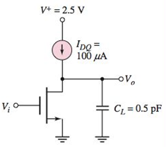
Figure P7.16
Want to see the full answer?
Check out a sample textbook solution
Chapter 7 Solutions
Microelectronics: Circuit Analysis and Design


- 7.65 In the circuit in Figure P7.65, the transistor parameters are: B = 120, VBE(on) = 0.7 V, VA = 100 V, C, = 1 pF, and fr = 600 MHz. (a) Deter- mine C, and the equivalent Miller capacitance CM. State any approxima- tions or assumptions that you make. (b) Find the upper 3 dB frequency and the midband voltage gain. Rc=D4 k2 R = 33 k2 C =1 uF Cc2 = 2 µF Rg = 2 k2 R = 5 ka R2 = 22 k2 Rg%3D 4 k2 Cg = 10 uF Figure P7.65 wwarrow_forward7.65 In the circuit in Figure P7.65, the transistor parameters are: B 120, Ver(on)=0.7 V, VA 100 V, C -I pF, and fr mine C, and the equivalent Miller capacitance Cy. State any approxima- tions or assumptions that you make. (b) Find the upper 3 dB frequency and the midband voltage gain. -600 MHz. (a) Deter- +5 V R= 33 ka wwHH Ry=22 k2 4 k2 10 wwarrow_forwardTYU 7.1 For the equivalent circuit shown in Figure 7.13, the parameters are: Rs = 1 k2, r, = 2 k2, RL = 4 k2, gm = 50 mA/V, and Cc 1 µF. (a) Determine the expression for the circuit time constant. (b) Calculate the 3 dB frequency and maximum gain asymptote. (c) Sketch the Bode plot of the transfer function magni- tude. (Ans. (a) t = (r+ Rs)Cc. (b) fsaB 53.1 Hz, [T (jo)Imax = 133) %3D %3D Rs Ce ww RL 8mVR Figure 7.13 Figure for Exercise TYU 7.1arrow_forward
- Q5. In the circuit in Figure P7.65, the transistor parameters are: B = 120, VBE (on) = 0.7 V, VA = 100 V, C, = 1 pF, and fr = 600 MHz. (a) Deter- mine C and the equivalent Miller capacitance CM. State any approxima- tions or assumptions that you make. (b) Find the upper 3 dB frequency and the midband voltage gain. +5 V Rc=4 k2 R = 33 k2 HH Cc2 = 2 µF CCi = 1 µF wwH Rs=2 kQ RL = 5 k2 R2 = 22 kO RE= 4 k2 CE= 10 µF Figure P7.65arrow_forward7.65 In the circuit in Figure P7.65, the transistor parameters are: B = 120, VBE(on) = 0.7 V, VA = 100 V, C, = 1 pF, and fr = 600 MHz. (a) Deter- mine C, and the equivalent Miller capacitance Cy. State any approxima- tions or assumptions that you make. (b) Find the upper 3 dB frequency and the midband voltage gain. +5 V Rc-4 k2 R= 33 k2 Ccz =2 AF CCi =1 uF wwwHE Rg = 2 ka 35 k2 R2= 22 ka 4 ks2 ww ww wwarrow_forwardIn the self-bias circuit of Figure 7.80 a. Draw the transfer characteristic curve of the device. b. Draw additional circuit equations on the same graph. Find c.lDQ and VGSQ. d. Calculate VDS , VD, VG, Vs. ...arrow_forward
- Problem 7.133(a): For the circuit shown below, let R1 = 106 kN, Rsig = 69 N, and RL Rsig. Assume that %3D 13 kN. Find the value of the bias current I in mA that results in Rin the source provides a small signal vsie and that B = 100. H RL R1 Rsig Ria 8arrow_forwardQ7. Figure Q7(a) shows the spectrum of a frequency modulated waveform with a sinusoidal modulation. 12 4.8 5.0 5.2 5.4 5.6 5.8 6.0 Frequency/MHz Figure Q7: (a) Spectrum of a frequency modulated waveform with a sinusoidal modulation. (a) Is this modulated waveform described as narrowband or as wideband? (b) What is the value of the carrier frequency? (c) What is the value of the modulation frequency? (d) Determine the value of the peak frequency deviation. Plots of Bessel functions of the first kind are provided below in Figure Q7(b) to assist you. (e) Estimate the fraction of the total signal power at the carrier frequency. (f) Detection of such a frequency modulated signal is usually accomplished with the use of a discriminator. Describe the function of a discriminator. (g) What is the equivalent AM modulation index obtained if this signal in Figure Q7(a) is demodulated with a high-pass RC filter discriminator? J„(x) 1.0 0.8 0.6 0.4 0.2 -0.2 -0.4 Figure Q7: (b) Bessel functions of the…arrow_forwardQ7. For the PMOS common-source circuit shown in Figure P7.69, the transistor parameters are: VTp = -2 V, K, Cgd = 3 pF. (a) Determine the upper 3 dB frequency. (b) What is the equiv- alent Miller capacitance? State any assumptions or approximations that you make. (c) Find the midband voltage gain. 1 mA/V², 1 = 0, Cgs = 15 pF, and +10 V Rs 0.5 kQ R=8 k2 Ci = 2 µF =Cs=10 µF wwHH R;=0.5 k2 Ce2 2 uF R3 = 22 k23 Rp=D 2 k2 RL= 5 k2 -10 V Figure P7.69 19 WW-arrow_forward
- a) Derive an expression for the circuit’s transfer function ?(??). b) Use the result from (a) to determine an equation for the cut-off frequency. c) Choose values for ? and ? that will yield a cut-off frequency of 15 ???.arrow_forwardA modulating signal f(t) has a maximum frequency of 18 kHz and peak value of 3volt, this signal is encoded using PCM. 1- Calculate the number of bits per sample if the number of levels is 130 2- Calculate the SNRQ if the average power of f(t) is 45 watt. 3- Calculate the minimum system bandwidth. e 7:20arrow_forwardDetermine the voltage gain plz λ is not 0 ..arrow_forward
 Introductory Circuit Analysis (13th Edition)Electrical EngineeringISBN:9780133923605Author:Robert L. BoylestadPublisher:PEARSON
 Delmar's Standard Textbook Of ElectricityElectrical EngineeringISBN:9781337900348Author:Stephen L. HermanPublisher:Cengage Learning
 Programmable Logic ControllersElectrical EngineeringISBN:9780073373843Author:Frank D. PetruzellaPublisher:McGraw-Hill Education
 Fundamentals of Electric CircuitsElectrical EngineeringISBN:9780078028229Author:Charles K Alexander, Matthew SadikuPublisher:McGraw-Hill Education
 Electric Circuits. (11th Edition)Electrical EngineeringISBN:9780134746968Author:James W. Nilsson, Susan RiedelPublisher:PEARSON
 Engineering ElectromagneticsElectrical EngineeringISBN:9780078028151Author:Hayt, William H. (william Hart), Jr, BUCK, John A.Publisher:Mcgraw-hill Education,