
Videos
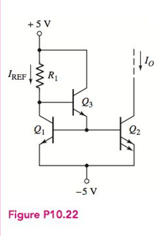
Consider the circuit in Figure P10.22. The transistor parameters for
Want to see the full answer?
Check out a sample textbook solution
Chapter 10 Solutions
Microelectronics: Circuit Analysis and Design


- 4. For the transistor in the figure shown below, the parameters are ß = 100 and VÀ = ∞. a. Design the circuit such that lEQ = 1mA and the Q-pt is in the center of the dc load line. b. If the peak-to-peak sinusoidal output voltage is 4V, determine the peak-to-peak sinusoidal signals at the base of the transistor and the peak-to-peak value of Vs. If the load resistor R₁ = 1kQ is connected to the output through a coupling capacitor, determine the peak-to-peak value in the output voltage, assuming vs is equal to the value determined in part (b). Vcc=+10 V www Rs = 0.7 kΩ Cc www RB RE voarrow_forwardQ.5. Consider the emitter-follower circuit shown in Figure below. Assume all transistors are matched with VB e(on) = 0.7 V, Vce(sat) = 0.2 V, and VA = ∞. Neglect the corresponding input voltages for the circuit to operate in the linear region. base currents. Determine the maximum and minimum values of output voltage and v+= 5 V R = 1 kQ R, = 1 kQ Q3 Q2 V- =-5 Varrow_forwardTime left 1:46:17 A bipolar junction transistor is described in the figure below. The transistor is implemented in the circuit with Vcc, Rc, and RB equal to 16 volts, 2k, and 10kn. Determine the value of Vout if Vin = 1.1V. V... in RB B Vec Ro V E outarrow_forward
- Q.1/ Figure below shows a CE power amplifier in which the collector resistor serves also as the load resistor. Assume Boc=Bac=100. a. Determines the de Q-point (Ico and VCEQ). b. Determine the voltage gain and the power gain. c. What changes would be necessary to convert the circuit to a pnp transistor with a positive supply? What advantage would this have? RL 100n 05 W LOk 22 uF RE 8.20 s00 mV pp 330 1O KHz 36 f1arrow_forwardcircuits by using the small signal models of the transistor. Assume the Early voltage of the transistors are infinitely large. Calculate the small-signal input and output impedances of the following Vcc R1 R1 Rout VB RE Rin R2arrow_forwardDesign a Common Emitter Voltage Divider Bias Amplifier circuit using. The current gain of the transistor chosen is typically 75 at a collector current of 10 mA. Use the supply voltage of 18 V and take the collector-emitter voltage at the Q- point to be half the supply voltage Information known at the Q-point: Vcc =18 V Ico = 10 mA VCEQ = 9 V Beta = 75 Calculate the value of the emitter resistor REQ:arrow_forward
- VBB RB ww IB Re IE Vcc The hybrid value of the transistor given in the figure is 50, the voltage values of V BB and V cc are 3V and 10V, respectively. Determine whether the transistor is in saturation, assuming the knee voltage value is 0.2 V, with the RB resistance 10 KQ and the R c resistance 1 KQ. (Note: Add your detailed solutions.)arrow_forwardIn reference to the given figure, VCB = 10.3V and VBE = 0.7V. NOTES: VCB = VC-VB VBE = VB-VE In reference to Figure 2, given the dc load line and the transistor circuit, what will be the value of RC, in kilo-ohms? In reference to Figure 2, given the dc load line and the transistor circuit, what will be the voltage of RB, in volts? In reference to Figure 2, given the dc load line and the transistor circuit, what will be the value of RB in kilo-ohms, if Beta=100?arrow_forward9. Design a biased-transistor circuit using VBB = Vcc= 10 V for a Q-point of Ic = 5 mA and VCE 4 V. Assume pc = 100. The design involves finding RB, RC, and the minimum power rating of the transistor. (The actual power rating should be greater.) Sketch the circuit.arrow_forward
- Q.5. Consider the emitter-follower circuit shown in Figure below. Assume all transistors are matched with VB Efon) = 0.7 V, VCEfsat) = 0.2 V, and VA = 00. Neglect base currents. Determine the maximum and minimum values of output voltage and the corresponding input voltages for the circuit to operate in the linear region. v* =5 V R =1 kQ -OvO R = 1 kQ Q2 V- =-5 V ww.arrow_forwardThe maximum values in the transistor circuit transferred to the side are given below. Maximum VCC voltage of BJT under normal conditionscalculate. PD(max)=24/100 W VCE(MAX)=20V IC(MAX)=100mA ßDC=150arrow_forwardFigure 1 2. For the class B output stage of Figure 2, let Vcc = 6 V and R, = 4N. If the output is a sinusoidal with 4.5V peak amplitude, find; (a) The output power. (b) The average power drawn from each supply/ (c) The power efficiency obtained at this output voltage. (d) The maximum power that each transistor must be capable of dissipating safely. +Vcc RL --Vcc Figure 2arrow_forward
 Introductory Circuit Analysis (13th Edition)Electrical EngineeringISBN:9780133923605Author:Robert L. BoylestadPublisher:PEARSON
 Delmar's Standard Textbook Of ElectricityElectrical EngineeringISBN:9781337900348Author:Stephen L. HermanPublisher:Cengage Learning
 Programmable Logic ControllersElectrical EngineeringISBN:9780073373843Author:Frank D. PetruzellaPublisher:McGraw-Hill Education
 Fundamentals of Electric CircuitsElectrical EngineeringISBN:9780078028229Author:Charles K Alexander, Matthew SadikuPublisher:McGraw-Hill Education
 Electric Circuits. (11th Edition)Electrical EngineeringISBN:9780134746968Author:James W. Nilsson, Susan RiedelPublisher:PEARSON
 Engineering ElectromagneticsElectrical EngineeringISBN:9780078028151Author:Hayt, William H. (william Hart), Jr, BUCK, John A.Publisher:Mcgraw-hill Education,