
Videos
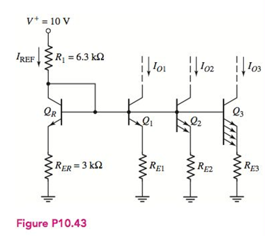
Consider the circuit in Figure P10.43. The transistor parameters are:
Want to see the full answer?
Check out a sample textbook solution
Chapter 10 Solutions
Microelectronics: Circuit Analysis and Design


- Q.1/ Figure below shows a CE power amplifier in which the collector resistor serves also as the load resistor. Assume Boc-Bac-100. a. Determines the de Q-point (Ico and VCEO). b. Determine the voltage gain and the power gain. c. What changes would be necessary to convert the circuit to a pnp transistor with a positive supply? What advantage would this have? +Vce +15 V R 100 LO K 0.5 W 22 juF RE 8.2 S00 mV pp 330 1 R 36 0 100 uFarrow_forwardcircuits by using the small signal models of the transistor. Assume the Early voltage of the transistors are infinitely large. Calculate the small-signal input and output impedances of the following Vcc R1 R1 Rout VB RE Rin R2arrow_forward32 The circuit shown in Figure P10.32 is a common-collector (also called an emitter follower) amplifier stage implemented with an npn silicon transistor. Determine VCEQ at the DC operating or Q point. Vcc = 12 V B = 130 R = 82 k2 R2 = 22 k2 Rs = 0.7 k2 Rp = 0.5 k2 RL = 16 2 R13 Vcl Rs R2 RE ww wwarrow_forward
- Q1. The output characteristic of a typical transistor is shown below, where the quiescent point is selected on it. This transistor is used in the bias circuit presented below. Find the suitable values of Rg and Rc to fix the Q-point of the circuit properly. +Vcc = 12 V 12- Is = 70 uA 10- Ig = 60 uA 8- Rc Is = 50 uA Rs 6- Ig= 40 uA 4. Is = 30 uĄ Is = 20 uA B = 100 2- VBE = 0.7 V 0- -2- 2 4 6 8 10 12 14 16 VCE (V) Ic (mA)arrow_forwardQ.5. Consider the emitter-follower circuit shown in Figure below. Assume all transistors are matched with VB e(on) = 0.7 V, Vce(sat) = 0.2 V, and VA = ∞. Neglect the corresponding input voltages for the circuit to operate in the linear region. base currents. Determine the maximum and minimum values of output voltage and v+= 5 V R = 1 kQ R, = 1 kQ Q3 Q2 V- =-5 Varrow_forwardConsider the circuit shown in figure, where VBE=700 mV, B = 100, and VA = co. Calculate the VCE of Q1. Assume that the emitter current is equal to collector current. Circuit parameters / - Rg = 140 kn, Rc = 0,7 kn, RE = 0,3 kn, Vcc = 12 V Vcc RB RC REarrow_forward
- 6. A BJT current source is designed as shown below, where QREF= Q₁. If IREF= 5 mA, determine Rp to have I₁= 2 mA (neglect the base current). 4. /REF QREF Vcc + Ка Rparrow_forward"It is desirable for the following circuit, assuming the transistors are the same." A) Common fashion gain B) Differential gain mode C) Input resistance network D) CMRR E) What effect does the change in load resistance have on the circuit? Vcc Rc Re Qu, Vi PEE -VEEarrow_forward1. For the circuit in Figure 1: a) Calculate the input and output power if the input signal results in a base current of 5 mA rms. b) Calculate the input power dissipated by the circuit if Rg is changed to 1.5 kN. c) What maximum output power can be delivered by the circuit if RB is changed to 1.5 kN? d) If the circuit is biased at its center voltage and center collector operating point, what is the input power for a maximum output power of 1.5 W? +Vcc (18 V) Rc = 16 2 RB 1.2 k2 V. B - 40 100 µF Figure 1arrow_forward
- Q.5. Consider the emitter-follower circuit shown in Figure below. Assume all transistors are matched with VB Efon) = 0.7 V, VCEfsat) = 0.2 V, and VA = 00. Neglect base currents. Determine the maximum and minimum values of output voltage and the corresponding input voltages for the circuit to operate in the linear region. v* =5 V R =1 kQ -OvO R = 1 kQ Q2 V- =-5 V ww.arrow_forwardFigure below shows a CE power amplifier in which the collector resistor serves also as the load resistor. Assume ßpc = Bac = 100, Determine- +Vcc +15V a. The de Q-point (Icq and VCEQ). b. The voltage gain and the power gain. RL 100n 0.5 W 1.0 kn c. The power dissipated in the transistor with no load d. the total power from the power supply with no load 22 uF e. the signal power in the load with a 500mV input Re 8.2 n 500 mV pp 1.0 kHz 330 n Rea 36 0 100 uFarrow_forwardFigure 1 2. For the class B output stage of Figure 2, let Vcc = 6 V and R, = 4N. If the output is a sinusoidal with 4.5V peak amplitude, find; (a) The output power. (b) The average power drawn from each supply/ (c) The power efficiency obtained at this output voltage. (d) The maximum power that each transistor must be capable of dissipating safely. +Vcc RL --Vcc Figure 2arrow_forward
 Introductory Circuit Analysis (13th Edition)Electrical EngineeringISBN:9780133923605Author:Robert L. BoylestadPublisher:PEARSON
 Delmar's Standard Textbook Of ElectricityElectrical EngineeringISBN:9781337900348Author:Stephen L. HermanPublisher:Cengage Learning
 Programmable Logic ControllersElectrical EngineeringISBN:9780073373843Author:Frank D. PetruzellaPublisher:McGraw-Hill Education
 Fundamentals of Electric CircuitsElectrical EngineeringISBN:9780078028229Author:Charles K Alexander, Matthew SadikuPublisher:McGraw-Hill Education
 Electric Circuits. (11th Edition)Electrical EngineeringISBN:9780134746968Author:James W. Nilsson, Susan RiedelPublisher:PEARSON
 Engineering ElectromagneticsElectrical EngineeringISBN:9780078028151Author:Hayt, William H. (william Hart), Jr, BUCK, John A.Publisher:Mcgraw-hill Education,