
Videos
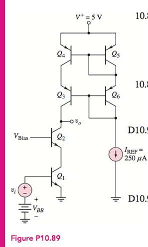
A BJT cascode amplifier with a cascode active load is shown inFigure P10.89. Assume transistor parameters of
The small-signal voltage gain
Answer to Problem 10.89P
Explanation of Solution
Given:
Calculation:
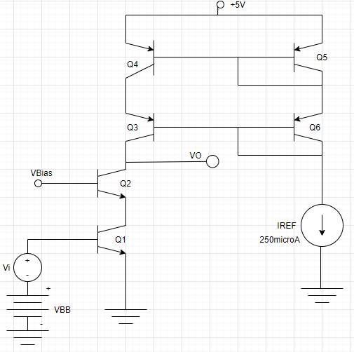
The given circuit is,
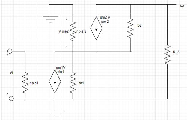
The equivalent circuit for active load amplifier is as shown,
The expression for input voltage
Now expression for output resistance is,
Put equation (3) in equation (2)
Consider
Now expression for hybrid resistor parameter.
Now output voltage will be,
Consider
Put value from equation (8) to equation (6)
Put
Now
Substitute the value for
Now
Substitute the derived values in equation (10)
Conclusion:
Want to see more full solutions like this?
Chapter 10 Solutions
Microelectronics: Circuit Analysis and Design


- Consider the MOSFET amplifer circuit shown in Figure below. Assume µnCox(W/L) = 4mA/V2, Vt = 1V Draw an equivalent DC model, and equivalent circuit of the amplifier. Determine the drain current and its overall voltage gain respectively.arrow_forwardQ4 Figure 4 shows a current mirror based on MOSFETS. Derive a formula relating the input current Iin to the output current Iout , and the output resistance, for the current mirror of Figure 4 stating any assumptions. (a) Iin Iout M1 M2 Vss = 0 V Figure 4 (b) Design a current mirror with improved output resistance and current balance using 4 NMOS transistors. Stating any assumption, derive the new output resistance and compare this with the current mirror in Figure 4. Why the output resistance value is important for a current mirror operation?arrow_forwardQ.2/ For the amplifier’s circuits shown below:a. Determine the Q-point for each amplifier circuit.b. What is the maximum peak value of collector current that can be realized in each circuit?c. What is the maximum peak value of output voltage in each circuit?arrow_forward
- Q.1/ Figure below shows a CE power amplifier in which the collector resistor serves also as the load resistor. Assume Boc-Bac-100. a. Determines the de Q-point (Ico and VCEO). b. Determine the voltage gain and the power gain. c. What changes would be necessary to convert the circuit to a pnp transistor with a positive supply? What advantage would this have? +Vce +15 V R 100 LO K 0.5 W 22 juF RE 8.2 S00 mV pp 330 1 R 36 0 100 uFarrow_forwardQUESTION 6: A simplified class-AB output stage with BJTs is shown below. The circuit parameters are Vcc= 23 V and R₁ = 1300 2. For each transistor, Is= 1 x 10 -15 A. Currents icnicp = 2 mA when v1 = 0. For vo= -5.1 V, determine it, ich, icp, and v₁. What is the power dissipated in On, Qp, and R₁ ? iz (mA) icn (mA) icp (mA) VI (V) Format: -9.3320876680856 Format: 6.0655035684487 Format: 5.9793972335256 Format: -8.5232348995442 Pon (mW) Format: 22.940360376887 Pop (mW) Format: 37.638052388388 PRL (MW) Format: 20.007968508449 VI VBB 2 VBB 2 + +Vcc 2n icn icp -V cc RL voarrow_forwardExplain how you can find the common emitter de current gain, B, and the common emitter ac current gain, hre, from the common emitter output characteristics of an npn transistor. You need to draw typical output characteristics in scales and provide numerical calculations to support your explanation.arrow_forward
- (1) Draw the circuit symbol for a NPN BJT. Label the terminals and currents. Chose the reference directions that agree with the true current directions for operation in the amplifier region. (2) Write the three working areas and the external bias conditions of the NPN BJT.arrow_forwardDesign a voltage divider biased CE stage with emitter degeneration. That stage should support a voltage gain of 5 and an input impedance larger than 3 KOhms with a bias current of 0.5 mA. Assume Beta=100, Is = 5e-17. Neglect the early voltage effect. You also need to provide values for the operating point of this transistor. Find the output resistance of this stage if the early voltage = 20 V.arrow_forwardRefer to the differential amplifier circuit shown below . Determine the quiescent DC voltage at the collector terminal of each transistor assuming VBE of two transistor are negligible. What will be the quiescent DC values if VBE is taken to be 0.7 V.arrow_forward
- Propose a suitable active load for a common collector amplifier configuration. Alsodefine what an active load is. How does the selected active load help improve the performancecharacteristics of the indicated amplifier stage? Explainarrow_forward2. You have two fixed bias circuits connected for testing. They are identical except that one is biased with a separate VBB source and the other is biased with the base resistor connected to Vcc. Ammeters are connected to measure collector current in each circuit. You vary the Vcc supply voltage and observe that the collector current varies in one circuit, but not in the other. In which circuit does the collector current change? Explain your observation.arrow_forwardQ) Choose (active, saturation or cutoff as the comver unewer for the following D When TaO and Ver Vea the transistor is operate in the. 2) When le is maximum and Ver minimum the traniistoris operate in the 31 The iransistir is operate as an amplifier in the region region region.arrow_forward
 Introductory Circuit Analysis (13th Edition)Electrical EngineeringISBN:9780133923605Author:Robert L. BoylestadPublisher:PEARSON
 Delmar's Standard Textbook Of ElectricityElectrical EngineeringISBN:9781337900348Author:Stephen L. HermanPublisher:Cengage Learning
 Programmable Logic ControllersElectrical EngineeringISBN:9780073373843Author:Frank D. PetruzellaPublisher:McGraw-Hill Education
 Fundamentals of Electric CircuitsElectrical EngineeringISBN:9780078028229Author:Charles K Alexander, Matthew SadikuPublisher:McGraw-Hill Education
 Electric Circuits. (11th Edition)Electrical EngineeringISBN:9780134746968Author:James W. Nilsson, Susan RiedelPublisher:PEARSON
 Engineering ElectromagneticsElectrical EngineeringISBN:9780078028151Author:Hayt, William H. (william Hart), Jr, BUCK, John A.Publisher:Mcgraw-hill Education,